
D2D Interface Bandwidth and Latency Comparison in Chiplet Architectures
Chiplet architecture has turned the package into a real performance battleground. Once multiple dies are placed side by side or stacked within the same advanced package, the quality of the die-to-die, or D2D, interface becomes one of the most important determinants of system behavior. Bandwidth is no longer a nice-to-have metric, and latency is no longer a small implementation detail. Together, they shape whether a chiplet system feels nearly monolithic or frustratingly fragmented.
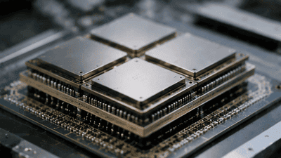
That is why comparing D2D interfaces through the lens of bandwidth and latency matters so much in advanced packaging and heterogeneous integration. Different interfaces offer different trade-offs in power, reach, cost, and design complexity. Some are built for ultra-high bandwidth in tightly coupled stacks. Others favor broader compatibility, easier integration, or lower energy per bit. In practice, chip architects must choose the right interface not by looking at one spec sheet, but by understanding how the whole package and system behave.
Why D2D Interfaces Became Central
The shift to chiplets began as a response to the limits of monolithic scaling. Large dies are expensive to manufacture, difficult to yield, and increasingly constrained by reticle size and routing congestion. By splitting functionality across multiple smaller dies, designers can improve yield, mix process nodes, and build more modular systems. But that only works if the chiplets can talk to each other fast enough and with low enough latency.
In older designs, communication across the package or board happened relatively slowly and with substantial overhead. Chiplets change the game because they are expected to communicate at speeds and latencies far closer to on-die interconnect than to traditional off-package links. That makes D2D interface design a core architectural decision. The interface has to preserve the advantages of partitioning without letting the system feel disjointed.
Advanced packaging makes this even more important because the physical distance between dies can be very small while the number of signals and the bandwidth demand can be huge. The package is no longer just a protective shell. It is the communication fabric.
Bandwidth vs. Latency: The Core Trade-Off

Bandwidth and latency often get discussed together, but they are not the same thing. Bandwidth is the amount of data that can move across the interface over time. Latency is the delay before data starts to move or before a response comes back. A D2D interface can have excellent bandwidth but still incur enough latency to hurt system performance if the protocol stack is heavy. Likewise, a low-latency link may not have enough raw bandwidth for memory-intensive workloads.
In chiplet systems, both matter. AI accelerators need huge bandwidth to move tensor data and memory traffic. CPUs and cache hierarchies care intensely about latency because they depend on fast synchronization and coherent access. Networking and signal-processing systems may need both: high throughput and rapid control-response behavior. That means no single D2D interface is universally best. The right answer depends on the workload.
It also depends on where the interface sits in the package. A very short, tightly controlled link on an interposer can support far higher effective bandwidth and lower latency than a longer or more complex package-level route. That is why advanced encapsulation is not just a packaging question. It is part of the interface budget.
Common D2D Interface Styles
Different chiplet ecosystems use different D2D interface styles, but most fall into a few broad categories. Some are standards-based and protocol-rich, while others are more specialized and optimized for raw performance.
Standardized protocol-based links
These interfaces often ride on familiar protocols such as PCIe or CXL, with adaptations for shorter package distances. Their advantage is interoperability. They can connect chiplets from different vendors or support a broader software ecosystem. Their drawback is that the protocol stack can add overhead, which may increase latency relative to a custom raw interface.
Raw, high-performance D2D links
These are optimized for very high bandwidth and low latency within a specific package or product family. They usually sacrifice some flexibility to achieve tighter timing, lower protocol overhead, and better power efficiency. They are common in tightly coupled AI and HPC systems where every cycle and every picojoule matter.
Bridge or interposer-based links
Some systems use silicon bridges or interposers to support D2D communication. These do not define the protocol themselves, but they make it possible to achieve dense routing, short paths, and high signal integrity. In many chiplet architectures, the quality of the bridge or interposer is as important as the interface protocol.
What Drives Bandwidth

Bandwidth in a D2D interface depends on several factors at once: lane count, signaling rate, encoding overhead, channel quality, and package topology. A link with many lanes can move more data, but it also consumes more area and power. A faster per-lane rate can raise throughput, but only if signal integrity remains intact.
This is where advanced packaging enters the picture. Shorter channels, better impedance control, and denser routing can raise usable bandwidth without requiring extreme power. Fine-pitch interconnects on an interposer or in a 3D stack can give chip architects a much larger beachfront bandwidth, meaning more throughput per unit width of package edge or interconnect area.
In practical terms, that makes the package itself a bandwidth multiplier. A chiplet link on an organic substrate may be perfectly usable, but the same interface on a silicon interposer or in a hybrid-bonded structure can look dramatically better. The physical packaging decision often determines the ceiling.
What Drives Latency
Latency is affected not only by signal travel time, but by the protocol layers above it. A short electrical path does not guarantee a short round-trip time if the interface has a long training sequence, heavy encoding, buffering, or complex flow control. That is why interface comparison must include both the PHY and the protocol stack.
Raw latency is often lowest in tightly integrated interfaces with minimal protocol overhead. These are the links used when chiplets behave like parts of a single coherent system rather than independent devices. Coherence traffic, cache access, and fine-grain synchronization all benefit from this style.
However, some amount of protocol overhead can be worth it if it brings flexibility or reliability. A more standardized D2D interface may have slightly higher latency, but it can simplify design reuse and allow broader ecosystem compatibility. Architects must decide whether the performance penalty is acceptable in exchange for portability and future proofing.
How Packaging Changes the Comparison
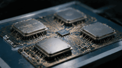
D2D interfaces do not live in isolation. Their performance is strongly shaped by advanced packaging choices such as 2.5D interposers, fan-out redistribution layers, and 3D bonding. A link that looks excellent on paper can underperform if the package introduces too much skew, loss, or routing congestion.
For example, in a 2.5D system with a silicon interposer, multiple chiplets can be placed close together with very short, dense connections. That boosts bandwidth and often lowers latency because the electrical path is short and controlled. In a fan-out package, the routing may be less dense but still efficient if the layout is optimized well. In a true 3D stack, vertical distance can be minimal, but thermal and mechanical challenges become much more serious.
This means interface choice and package choice are inseparable. A chip architect who evaluates D2D links without considering the package is only seeing half the system. Advanced encapsulation is the other half.
Latency-Sensitive vs. Bandwidth-Sensitive Workloads
Not all chiplet systems care about D2D performance in the same way. Some are mostly bandwidth-driven. Others are mostly latency-driven. Many are both, but in different proportions.
AI accelerators often lean heavily toward bandwidth. Large matrix operations move vast quantities of data between compute and memory, so the key question is whether the package can deliver enough throughput without wasting too much power. Latency still matters, but it is usually secondary to raw data movement.
CPU chiplet systems often care much more about latency. Cache coherency, inter-core communication, and memory access behavior all depend on quick responses. In that world, a lower-latency D2D interface can improve real-world performance even if bandwidth is not the primary bottleneck.
Networking and control-heavy systems sit somewhere in between. They may need bursts of high bandwidth, but they also need quick control signaling. That is why a one-dimensional comparison does not work well. The best interface is the one that matches the workload profile.
Power Efficiency Is Part of the Story
Bandwidth and latency are only two of the axes in D2D interface comparison. Power per bit is another major factor, and in many chiplet architectures it matters just as much. A link that delivers high bandwidth but consumes too much energy can quickly become unattractive, especially in AI and mobile-class systems.
Advanced packaging helps here by shortening the channel and improving signal quality. That can reduce the energy required per transmitted bit. Some interfaces use very efficient signaling and lower overhead to keep pJ/bit down. Others rely on physical proximity and dense routing to maintain performance without requiring large swings or complex retransmissions.
This is one of the reasons chip architects increasingly consider bandwidth, latency, and energy together. They are all part of the same trade space. A few extra cycles of latency may be acceptable if the link is dramatically more energy-efficient, but that depends on the system-level goal.
Standards vs. Custom Links
The D2D landscape is also shaped by the tension between standardized interfaces and custom links. Standards are attractive because they promote interoperability and ecosystem growth. They can make it easier to mix chiplets from different vendors or reuse designs across generations. But standardization can add layers of abstraction that increase latency or limit optimization.
Custom links, by contrast, can be tuned very aggressively for the package and workload at hand. They may deliver superior bandwidth and lower latency because they avoid unnecessary generality. But they often lock the system into a specific vendor or product family, which reduces flexibility.
This is where many chiplet architects land in the middle. They may use a standardized interface for broader interoperability and a custom high-performance link for the most critical internal connections. That hybrid strategy is common in advanced packaging because the package itself can support multiple interconnect flavors in one system.
Measurement Is Harder Than It Looks
Comparing D2D interface bandwidth and latency sounds straightforward, but it becomes tricky in real hardware. Different measurement methods can produce different results. Are you measuring raw PHY throughput or effective payload bandwidth? Are you looking at one-way latency, round-trip latency, or application-level response time? Are you measuring at nominal conditions or across process-voltage-temperature corners?
The package also matters. A link’s behavior can change depending on the substrate, interposer, die spacing, and whether the system uses 2.5D or 3D integration. A comparison that ignores those variables may be useful for marketing, but not for real design decisions.
That is why serious chiplet design teams often build cross-layer models that combine package physics, protocol behavior, and workload characteristics. You cannot design a good D2D interface in isolation anymore. You have to model the entire stack.
How Architects Decide
When choosing a D2D interface, chip architects usually ask a few practical questions:
- How much bandwidth does the workload really need?
- How sensitive is the system to latency?
- How much power can the package afford to spend per bit?
- Does the design require interoperability or is it a closed platform?
- What kind of package technology will support the link best?
Those questions often lead to a layered answer. A high-end AI package may use a very fast, low-latency internal link between compute chiplets and memory-related chiplets, while also supporting a more standardized path for peripheral or management functions. A CPU complex may prioritize coherence latency but accept moderate bandwidth. A modular system may trade some raw performance for ecosystem flexibility.
There is rarely a perfect answer. There is only the best compromise for the system in front of you.
Where the Field Is Heading
The future of D2D interfaces will likely be shaped by two parallel forces: tighter integration and broader standardization. On one side, advanced packaging will keep shrinking the physical distance between dies, allowing even lower latency and higher bandwidth. On the other side, the industry will continue to seek common interfaces that make chiplet ecosystems easier to scale.
We are likely to see more mixed-interface packages, where some links are ultra-fast and custom while others are standardized and flexible. We will also see more co-design between D2D protocol developers and packaging engineers, because the best interface is increasingly determined by the available package architecture.
Eventually, D2D comparison may look less like “which interface is fastest” and more like “which interface best matches this workload, this package, and this business model.” That is a more mature way to think about it, and a better one.
Conclusion
Bandwidth and latency are the two most visible measures of D2D interface quality, but they only make sense in context. In chiplet architectures, those metrics are shaped by advanced packaging, heterogeneous integration, protocol overhead, power efficiency, and the physical design of the package itself. The best interface is not the one with the biggest numbers in isolation. It is the one that lets the system behave like a well-designed whole.
That is why D2D interface comparison has become such an important topic in advanced encapsulation. As chiplets spread across AI, HPC, networking, and consumer products, the package is turning into a real architectural battlefield. In that battlefield, bandwidth gets the headlines, latency keeps the system responsive, and the packaging layer quietly decides how much of either you can actually use.





